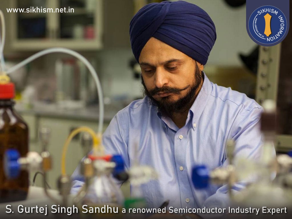
Dr. Gurtej Singh Sandhu
Gurtej Sandhu is Senior Fellow and Vice President at Micron Technology. In his current role, he is responsible for Micron’s end-to-end (Si-to-Package) R&D technology roadmaps. The scope includes driving cross-functional alignment across various departments and business units to proactively identify technology gaps, and managing the engineering organization to resource and execute on developing innovative technology solutions for future memory scaling. Dr. Sandhu’s responsibilities include leading several internal project teams worldwide and managing interactions with research consortia around the world.
At Micron, Dr. Sandhu has held several engineering and management roles. He has been actively involved with a broad range of process technologies for IC processing and has pioneered several process technologies currently employed in mainstream semiconductor chip manufacturing.
Dr. Sandhu received a degree in electrical engineering at the Indian Institute of Technology, New Delhi, and a Ph.D. in physics at the University of North Carolina, Chapel Hill, in 1990. He holds over 1,300 U.S. patents and is recognized as one of the top inventors in the world. Dr. Sandhu is a Fellow of IEEE. In 2018, he received the IEEE Andrew S. Grove Award for outstanding contributions to silicon CMOS process technology that enables DRAM and NAND memory chip scaling.
Gurtej Singh Sandhu, also known as Gurtej Sandhu, is an inventor in the fields of thin-film processes and materials, VLSI and semiconductor device fabrication. He is recognized for being the all-time seventh most prolific inventor as measured by number of U.S. utility patents. Gurtej has 1382 U.S. utility patents as of October 19, 2021. He was Senior Fellow and Director of Advanced Technology Developments at Micron Technology, before becoming Senior Fellow and Vice President of Micron Technology.
The publication Kiplinger reports, "Sandhu developed a method of coating microchips with titanium without exposing the metal to oxygen, which would ruin the chips. Initially, he didn't think his idea was a big deal, but now most memory-chip makers use the process." The publication also states that Gurtej earned an electrical engineering degree at the Indian Institute of Technology – Delhi in India and a physics PhD at the University of North Carolina at Chapel Hill.
The Institute of Electrical and Electronics Engineers (IEEE) awarded Sandhu the 2018 IEEE Andrew S. Grove Award for outstanding contributions to solid-state devices and technology. They said his "pioneering achievements concerning patterning and materials integration have enabled the continuation of Moore’s Law for aggressive scaling of memory chips integral to consumer electronics products such as cell phones, digital cameras and solid-state drives for personal and cloud server computers." The IEEE states: "Sandhu initiated the development of atomic layer deposition high-κ films for DRAM devices and helped drive cost-effective implementation starting with 90-nm node DRAM. Extreme device scaling was also made possible through his pitch-doubling process, which led to the first 3X-nm NAND flash memory. Sandhu’s method for constructing large-area straight-wall capacitors enabled the formation of double-sided capacitors that extended the scaling of important one-transistor, one-capacitor (1T1C) device technologies. His process for CVD Ti/TiN is still in use for making DRAM and NAND chips."
Gurtej Singh Sandhu is a Prolific Inventor and has the record of the highest number of patents ever issued to a person of Indian origin. Gurtej has 1375 patents and works at Micron.
Records held by Gurtej Singh Sandhu:
Highest number of patents ever issued to a person of Indian origin (see complete list) 6th Highest number of patents ever issued to an person (Worldwide)
Name: Gurtej Singh Sandhu
Patents: 1375
Associated: Micron Technology
First patent on: 1991
Education: PhD (Electrical Engineering)
B. Tech in Electrical Engineering from Indian Institute of Technology, Delhi (IIT, Delhi) PhD in Electrical Engineering from University of North Carolina, Chapel Hill Award: IEEE Andrew S. Grove Award in 2018 He is a notable employee of Micron Technology, a company developing Computer memory and data storage devices such as RAM and USB. He was a major player in driving the growth of Micron in early 2000s.
Background of Gurtej Singh Sandhu Gurtej Singh Sandhu was born in London (in 24th October 1960) to parents of Indian origin (Sarjit Sandhu and Gurmit Sandhu) and moved to India at the age of 3 years in 1963.
He completed in Bachelors' degree in India from Indian Institute of Technology, Delhi following which he moved to United States of America (USA). IIT, Delhi is known to be one of the best premium Engineering Institute in India ranking in top 3 nationally.
He moved in USA in 1985.
Gurtej completed his PhD in Electrical Engineering from University of North Carolina, Chapel Hill.
Initially, Gurtej's career has been as follows:
Process development engineer at Micron Technology (1989-1991) Senior engineer at Micron Technology (1991-1993) Section head at Micron Technology (1993) Currently, Gurtej works as Senior Fellow and Director of Technology Development at Micron Technology, USA.
From a personal point of view, Gurtej got married in 21st June 1987 and has 2 children.
He is associated with Guru Nanak Dev University (GNDU), Amritsar and helps in running the University founded in 2007.
Patents by Gurtej Singh Sandhu
Gurtej Singh Sandhu holds the record for the most patents by an Indian. He has over 1340 utility patents and is Senior Fellow and Vice President at Micron Technology. He works in the field of Electrical Engineering.
Gurtej's first patent was in 1991 at the age of 31.
Gurtej's research focus is on:
Thin film processing VLSI and semiconductor device fabrication Significant contributions by Gurtej Singh Sandhu:
Started development of atomic layer deposition high-k films for DRAM devices at Micron in 2000 along with Trung T. Doan Helped initiate cost effective implementation of 90 nanometer node DRAM Developed a pitch doubling process which made it possible for high device scaling His inventions resulted in 3X nanometer NAND flash memory Developed method for constructing large area straight wall capacitors His methods for CVD Ti/TiNi is used in making DRAM and NAND industry wide. He is a notable researcher in this field.
Some Example patents by Gurtej Singh Sandhu:
Resonator for thermo optic device Chemical vapor deposition of titanium Waveguide for thermo optic device Enhanced atomic layer deposition Resistive heater for thermo optic device Process for growing a dielectric layer on a silicon-containing surface using a mixture of NO and O Atomic layer deposition and conversion Small grain size, conformal aluminum interconnects and method for their formation Memory device with chemical vapor deposition of titanium for titanium silicide contacts Apparatus having a titanium alloy layer Use of DAR coating to modulate the efficiency of laser fuse blows Conductive container structures having a dielectric cap Chemical vapor deposition of titanium Slurry with chelating agent for chemical-mechanical polishing of a semiconductor wafer and methods related thereto Methods of forming a contact having titanium formed by chemical vapor deposition DRAM and NAND memory chip scaling A method to coat microchips with titanium without exposing the metal to oxygen Method to develop atomic layer deposition high-k films for DRAM devices All Patent by Gurtej Singh Sandhu on USPTO.